(Hong Kong)


Product Summary
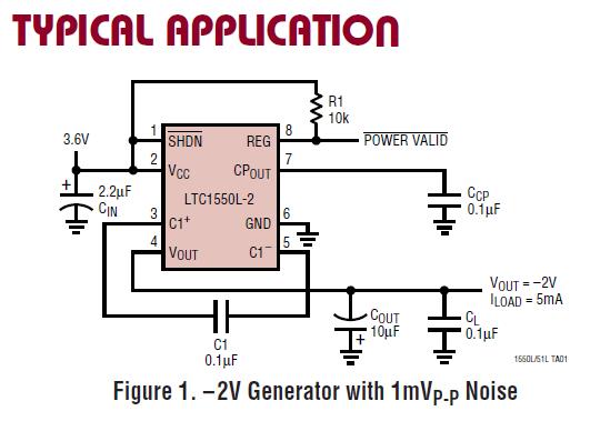
The LTC1550LIGN#TR is a switched capacitor charge pump voltage inverter which includes internal linear post-regulators to minimize output ripple. Output voltages are fixed at -4.1V, -2.5V and -2V with ripple voltages typically below 1mVP-P. The LTC1550LIGN#TR is also available in an adjustable output voltage version. The device is ideal for use as bias voltage generators for GaAs transmitter FETs in portable RF and cellular telephone applications. The applications of the LTC1550LIGN#TR include GaAs FET Bias Generators, Negative Supply Generators, Battery-Powered Systems, Single Supply Applications.
Parametrics
LTC1550LIGN#TR absolute maximum ratings: (1)Supply Voltage: 5.5V; (2)Output Voltage: 0.3V to (VCC - 10.5V); (3)Total Voltage, VCC to CPOUT: 10.8V; (4)Input Voltage (SHDN Pin): -0.3V to (VCC + 0.3V); (5)Input Voltage (REG Pin): -0.3V to 6V; (6)Output Short-Circuit Duration: 30 sec; (7)Commercial Temperature Range: 0℃ to 70℃; (8)Extended Commercial Operating, Temperature Range (Note 3): -40℃ to 85℃; (9)Industrial Temperature Range: -40℃ to 85℃; (10)Storage Temperature Range: -65℃ to 150℃; (11)Lead Temperature (Soldering, 10 sec): 300℃.
Features
LTC1550LIGN#TR features: (1)Regulated Negative Voltage from a Single Positive Supply; (2)Low Output Ripple: Less Than 1mVP-P Typ; (3)High Charge Pump Frequency: 900kHz Typ; (4)Small Charge Pump Capacitors: 0.1mF; (5)Requires Only Four External Capacitors; (6)Fixed -4.1V or Adjustable Output; (7)Shutdown Mode Drops Supply Current to < 1mA; (8)High Output Current: Up to 10mA, VCC = 5V; (9)Output Regulation: 5%; (10)Available in SO-8 and 16-Lead SSOP.
Diagrams
| Image | Part No | Mfg | Description |  |
Pricing (USD) |
Quantity | ||||||
|---|---|---|---|---|---|---|---|---|---|---|---|---|
 |
 LTC1550LIGN#TR |
|
IC REG SWITCHED CAP INV 16SSOP |
Data Sheet |
|
|
||||||
|
LTC1550LIGN#TRPBF |
|
IC REG SWITCHED CAP INV 16SSOP |
Data Sheet |
|
|
||||||