Product Summary
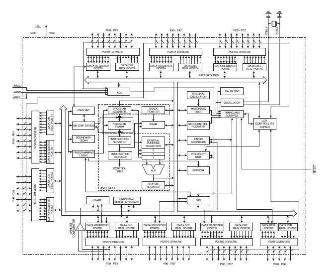
The ATMEGA329PV-10AU is an 8-bit Microcontroller with In-System Programmable Flash. The ATMEGA329PV-10AU combines a rich instruction set with 32 general purpose working registers. All the 32 registers are directly connected to the Arithmetic Logic Unit (ALU), allowing two independent registers to be accessed in one single instruction executed in one clock cycle. The resulting architecture is more code efficient while achieving throughputs up to ten times faster than conventional CISC microcontrollers. The ATMEGA329PV-10AUprovides the following features: 32/64K bytes of In- System Programmable Flash with Read-While-Write capabilities, 1/2K bytes EEPROM, 2/4K byte SRAM, 54/69 general purpose I/O lines, 32 general purpose working registers, a JTAG interface for Boundary-scan, On-chip Debugging support and programming, a complete On-chip LCD controller with internal contrast control, three flexible Timer/Counters with compare modes, internal and external interrupts, a serial programmable USART, Universal Serial Interface with Start Condition Detector, an 8- channel, 10-bit ADC, a programmable Watchdog Timer with internal Oscillator, an SPI serial port, and five software selectable power saving modes. The Idle mode stops the CPU while allowing the SRAM, Timer/Counters, SPI port, and interrupt system to continue functioning.
Parametrics
ATMEGA329PV-10AU absolute maximum ratings: (1)Operating Temperature: -55℃ to +125℃; (2)Storage Temperature: -65℃ to +150℃; (3)Voltage on any Pin except RESET with respect to Ground: -0.5V to VCC+0.5V; (4)Voltage on RESET with respect to Ground: -0.5V to +13.0V; (5)Maximum Operating Voltage: 6.0V; (6)DC Current per I/O Pin: 40.0 mA; (7)DC Current VCC and GND Pins: 200.0 mA.
Features
ATMEGA329PV-10AU features: (1)130 Powerful Instructions Most Single Clock Cycle Execution; (2)32 x 8 General Purpose Working Registers; (3)Boundary-scan Capabilities According to the JTAG Standard; (4)Extensive On-chip Debug Support; (5)Programming of Flash, EEPROM, Fuses, and Lock Bits through the JTAG Interface; (6)Real Time Counter with Separate Oscillator; (7)Four PWM Channels; (8)8-channel, 10-bit ADC; (9)Programmable Serial USART; (10)Master/Slave SPI Serial Interface; (11)Universal Serial Interface with Start Condition Detector; (12)Programmable Watchdog Timer with Separate On-chip Oscillator; (13)On-chip Analog Comparator; (14)Interrupt and Wake-up on Pin Change; (15)Power-on Reset and Programmable Brown-out Detection; (16)Internal Calibrated Oscillator; (17)External and Internal Interrupt Sources.
Diagrams
| Image | Part No | Mfg | Description |  |
Pricing (USD) |
Quantity | ||||||||||||
|---|---|---|---|---|---|---|---|---|---|---|---|---|---|---|---|---|---|---|
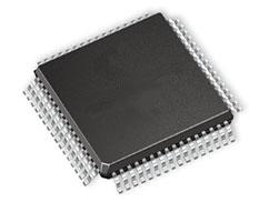 |
 ATMEGA329PV-10AU |
 Atmel |
 8-bit Microcontrollers (MCU) AVR 32K FLSH 2K SRAM 1KB EE-10 MHZ 1.8V |
 Data Sheet |

|
|
||||||||||||
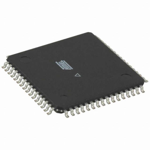 |
 ATMEGA329PV-10AUR |
 Atmel |
 8-bit Microcontrollers (MCU) AVR 32K FLSH 2K SRAM 1KB EE-10MHZ 1.8V |
 Data Sheet |

|
|
||||||||||||
 (Hong Kong)


