(Hong Kong)


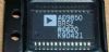
Product Summary
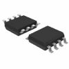
The MC100LVEL11DR2 is a differential 1:2 fanout buffer. The device is functionally similar to the E111 device but with higher performance capabilities. Having within-device skews and output transition times significantly improved over the E111, the LVEL11 is ideally suited for those applications which require the ultimate in AC performance. The MC100LVEL11DR2 employs clamping circuitry to maintain stability under open input conditions. If the inputs are left open (pulled to VEE) the Q outputs will go LOW.
Parametrics
MC100LVEL11DR2 absolute maximum ratings: (1)VCC PECL Mode Power Supply VEE = 0 V: 8 to 0 V; (2)VEE NECL Mode Power Supply VCC = 0 V: -8 to 0 V; (3)VI PECL Mode Input Voltage VEE = 0 V VI ≤ VCC: 6 to 0V; (4)NECL Mode Input Voltage VCC = 0 V VI ≤ VEE: -6 to 0V; (5)Iout Output Current Continuous: 50mA; (6)Iout Output Current Surge: 100mA; (7)TA Operating Temperature Range: -40 to +85℃; (8)Tstg Storage Temperature Range: -65 to +150℃; (9)θJA Thermal Resistance (Junction to Ambient): 0 lpfm 190℃/W, 500 lpfm 130℃/W; (10)θJC Thermal Resistance (Junction to Case) Standard Board: 41 to 44 ± 5% ℃/W; (11)θJA Thermal Resistance (Junction to Ambient): 0 lpfm 185℃/W, 500 lpfm 140℃/W; (12)θJC Thermal Resistance (Junction to Case) Standard Board: 41 to 44 ± 5% ℃/W; (13)θJA Thermal Resistance (Junction to Ambient): 0 lfpm 129℃/W, 500 lfpm 84℃/W; (14)Tsol Wave Solder Pb <2 to 3 sec @ 248℃: 265℃; (15)Tsol Wave Solder Pb-Free <2 to 3 sec @ 260℃: 265℃.
Features
MC100LVEL11DR2 features: (1)330 ps Propagation Delay; (2)5 ps Skew Between Outputs; (3)High Bandwidth Output Transitions; (4)The 100 Series Contains Temperature Compensation; (5)PECL Mode Operating Range: VCC = 3.0 V to 3.8 V with VEE = 0 V; (6)NECL Mode Operating Range: VCC = 0 V with VEE = -3.0 V to -3.8 V; (7)Internal Input Pulldown Resistors; (8)Q Output will Default LOW with Inputs Open or at VEE; (9)Pb-Free Packages are Available.
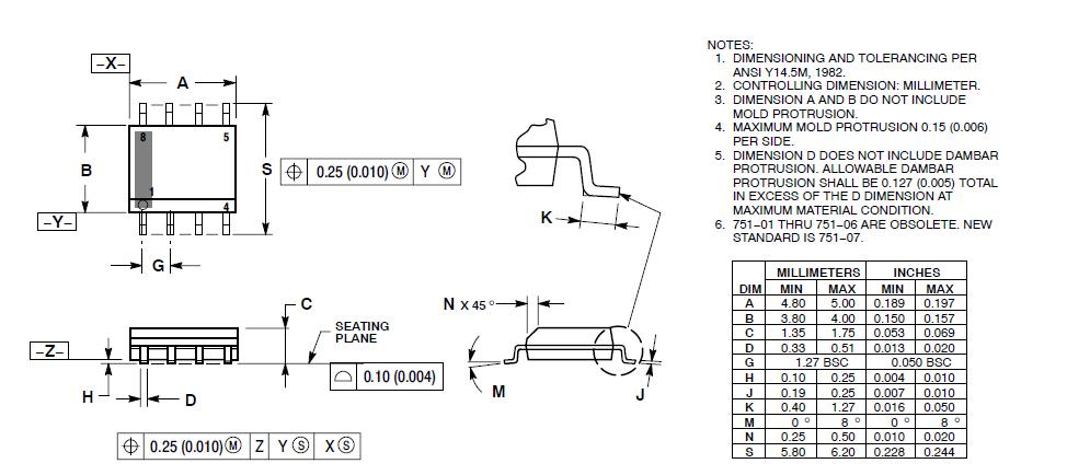
Diagrams
| Image | Part No | Mfg | Description |  |
Pricing (USD) |
Quantity | ||||||||||
|---|---|---|---|---|---|---|---|---|---|---|---|---|---|---|---|---|
 |
 MC100LVEL11DR2 |
ON Semiconductor |
Clock Buffer 3.3V ECL 1:2 Diff |
Data Sheet |
Negotiable |
|
||||||||||
|
MC100LVEL11DR2G |
ON Semiconductor |
Clock Buffer 3.3V ECL 1:2 Diff Fanout Buffer |
Data Sheet |
|
|
||||||||||