(Hong Kong)


Product Summary
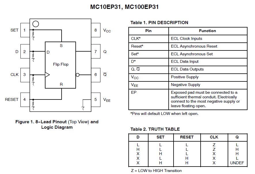
The MC10EP31DR2 is a D flip-flop with set and reset. The device is pin and functionally equivalent to the EL31 and LVEL31 devices. With AC performance much faster than the EL31 and LVEL31 devices, the MC10EP31DR2 is ideal for applications requiring the fastest AC performance available. Both set and reset inputs are asynchronous, level triggered signals. Data enters the master portion of the flip-flop when CLK is low and is transferred to the slave, and thus the outputs, upon a positive transition of the CLK.
Parametrics
MC10EP31DR2 absolute maximum ratings: (1)VCC PECL Mode Power Supply VEE = 0 V: 6 V; (2)VEE NECL Mode Power Supply VCC = 0 V: -6 V; (3)VI PECL Mode Input Voltage VEE = 0 V VI ≤ VCC: 6V; (4)NECL Mode Input Voltage VCC = 0 V VI ≥ VEE: -6V; (5)Iout Output Current Continuous: 50mA; (6)Iout Output Current Surge: 100mA; (7)IBB VBB Sink/Source: ± 0.5 mA; (8)TA Operating Temperature Range: -40 to +85 ℃; (9)Tstg Storage Temperature Range: -65 to +150 ℃; (10)θJA Thermal Resistance (Junction to Ambient): 0 lfpm 190℃/W, 500 lfpm 130℃/W; (11)θJC Thermal Resistance (Junction to Case) Standard Board: 41 to 44 ℃/W; (12)Tsol Wave Solder Pb <2 to 3 sec @ 248℃: 265℃; (13)Tsol Wave Solder Pb- Free <2 to 3 sec @ 260℃: 265℃.
Features
MC10EP31DR2 features: (1)340 ps Typical Propagation Delay; (2)Maximum Frequency > 3 GHz Typical; (3)PECL Mode Operating Range: VCC = 3.0 V to 5.5 V with VEE = 0 V; (4)NECL Mode Operating Range: VCC = 0 V with VEE = -3.0 V to -5.5 V; (5)Open Input Default State; (6)Q Output Will Default LOW with Inputs Open or at VEE; (7)Pb-Free Packages are Available.
Diagrams
| Image | Part No | Mfg | Description |  |
Pricing (USD) |
Quantity | ||||||||||
|---|---|---|---|---|---|---|---|---|---|---|---|---|---|---|---|---|
 |
 MC10EP31DR2 |
ON Semiconductor |
Flip Flops 3.3V/5V ECL D-Type |
Data Sheet |
Negotiable |
|
||||||||||
|
MC10EP31DR2G |
ON Semiconductor |
Flip Flops 3.3V/5V ECL D-Type w/Set and Reset |
Data Sheet |
|
|
||||||||||