(Hong Kong)


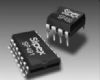
Product Summary
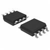
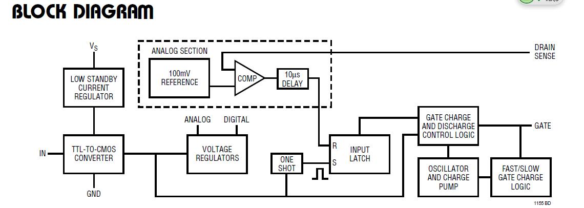
The LTC1155CS8#TR is a dual high side gate driver which allows using low cost N-channel FETs for high side switching applications. An internal charge pump boosts the gate above the positive rail, fully enhancing an N-channel MOSFET with no external components. Micropower operation, with 8μA standby current and 85μA operating current, allows use in virtually all systems with maximum efficiency. Included on-chip is overcurrent sensing to provide automatic shutdown in case of short circuits. A time delay can be added in series with the current sense to prevent false triggering on high in-rush loads such as capacitors and incandescent lamps. The LTC1155CS8#TR operates off of a 4.5V to 18V supply input and safely drives the gates of virtually all FETs. The LTC1155CS8#TR is well suited for low voltage (battery-powered) applications, particularly where micropower "sleep" operation is required. The LTC1155CS8#TR is available in 8-pin SO package.
Parametrics
LTC1155CS8#TR absolute maximum ratings: (1)Supply Voltage: 22V; (2)Input Voltage: (VS +0.3V) to (GND – 0.3V); (3)Gate Voltage: (VS +24V) to (GND – 0.3V); (4)Current (Any Pin): 50mA; (5)Storage Temperature Range: – 65℃ to 150℃; (6)Operating Temperature Range: 0℃ to 70℃; (7)Lead Temperature Range (Soldering, 10 sec.): 300℃.
Features
LTC1155CS8#TR features: (1)Fully Enhances N-Channel Power MOSFETs; (2)8μA Standby Current; (3)85μA ON Current; (4)Short-Circuit Protection; (5)Wide Power Supply Range: 4.5V to 18V; (6)Controlled Switching ON and OFF Times; (7)No External Charge Pump Components; (8)Replaces P-Channel High Side MOSFETs; (9)Compatible with Standard Logic Families; (10)Available in 8-Pin SO Package.
Diagrams
| Image | Part No | Mfg | Description |  |
Pricing (USD) |
Quantity | ||||||
|---|---|---|---|---|---|---|---|---|---|---|---|---|
 |
 LTC1155CS8#TR |
|
IC DRIVER MOSF HISIDE DUAL 8SOIC |
Data Sheet |
|
|
||||||
|
LTC1155CS8#TRPBF |
|
IC MOSFET DVR HI-SIDE DUAL 8SOIC |
Data Sheet |
|
|
||||||