(Hong Kong)


Product Summary
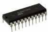
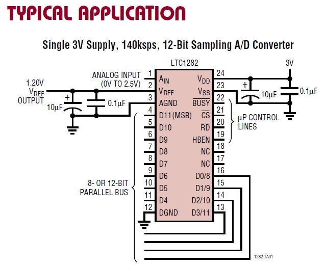
The LTC1282BCSW#TR is a 6ms, 140ksps, sampling 12-bit A/D converter that draws only 12mW from a single 3V or dual ±3V supply. This easy-to-use device comes complete with 1.14ms sample-and-hold, precision reference and internally trimmed clock. Unipolar and bipolar conversion modes provide flexibility for various applications. The device is built with LTBiCMOSTM switched capacitor technology. The applications of the LTC1282BCSW#TR include 3V Powered Systems, High Speed Data Acquisition, Digital Signal Processing, Multiplexed Data Acquisition Systems, Audio and Telecom Processing, Spectrum Analysis.
Parametrics
LTC1282BCSW#TR absolute maximum ratings: (1)Supply Voltage (VDD): 12V; (2)Negative Supply Voltage (VSS): -6V to GND; (3)Total Supply Voltage (VDD to VSS): 12V; (4)Analog Input Voltage: VSS -0.3V to VDD + 0.3V; (5)Digital Input Voltage: VSS -0.3V to 12V; (6)Digital Output Voltage: VSS -0.3V to VDD + 0.3V; (7)Power Dissipation: 500mW; (8)Specified Temperature Range: 0℃ to 70℃; (9)Operating Temperature Range: 0℃ to 70℃; (10)Storage Temperature Range: -65℃ to 150℃; (11)Lead Temperature (Soldering, 10 sec): 300℃.
Features
LTC1282BCSW#TR features: (1)Single Supply 3V or ±3V Operation; (2)140ksps Throughput Rate; (3)12mW (Typ) Power Dissipation; (4)On-Chip 25ppm/℃ Reference; (5)Internal Synchronized Clock; No Clock Required; (6)High Impedance Analog Input; (7)69dB S/(N + D) and 77dB THD at Nyquist; (8)±0.5LSB INL and ±0.75LSB DNL Max (A Grade); (9)2.7V Guaranteed Minimum Supply Voltage; (10)ESD Protected On All Pins; (11)24-Pin Narrow PDIP and SW Packages; (12)0V to 2.5V or ±1.25V Input Ranges.
Diagrams
| Image | Part No | Mfg | Description |  |
Pricing (USD) |
Quantity | ||||||
|---|---|---|---|---|---|---|---|---|---|---|---|---|
 |
 LTC1282BCSW#TR |
|
IC ADC 12BIT SAMPLING REF 24SOIC |
Data Sheet |
|
|
||||||
|
LTC1282BCSW#TRPBF |
|
IC A/D CONV SAMPLING W/REF24SOIC |
Data Sheet |
|
|
||||||