(Hong Kong)


Product Summary
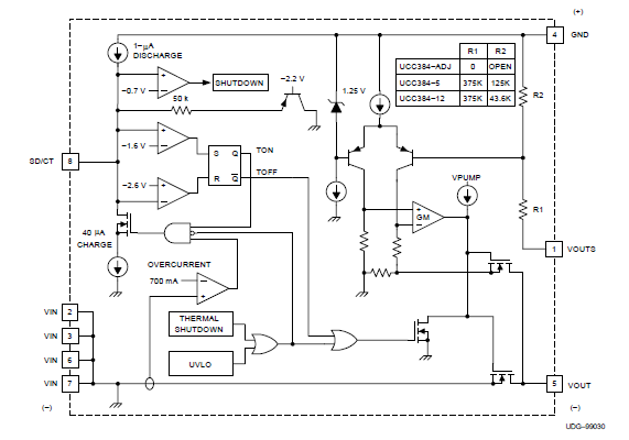
The UCC384DP-ADJ is a negative linear-series pass regulator which is tailored for low-dropout applications where low-quiescent power is important. Fabricated with a BCDMOS technology ideally suited for low input-to-output differential applications, the UCC384DP-ADJ passes 0.5 A while requiring only 0.2 V of input-voltage headroom. Dropout voltage decreases linearly with output current, so that dropout at 50 mA is less than 20 mV. Quiescent current consumption for the device under normal (non-dropout) conditions is typically 200 μA. An integrated charge pump is internally enabled only when the device is operating near dropout with low VIN. This ensured that the UCC384DP-ADJ meets the dropout specifications even for maximum load current and a VIN of –3.2 V with only a modest increase in quiescent current. Quiescent current is always less than 350 μA, with the charge pump enabled. The quiescent current of the UCC384DP-ADJ does not increase with load current. Short-circuit current is internally limited. The device responds to a sustained overcurrent condition by turning off after a tON delay. The UCC384DP-ADJ then stays off for a period, tOFF, that is 40 times the tON delay. The device then begins pulsing on and off at the tON/tOFF duty cycle of 2.5%. This drastically reduces the power dissipation during short circuit such that heat sinking, if at all required, must only accommodate normal operation. An external capacitor sets the on time. The off time is always 40 times tON. The UCC384DP-ADJ can be shutdown to 45 μA (maximum) by pulling the SD/CT pin more positive than –0.7 V. To allow for simpler interfacing, the SD/CT pin may be pulled up to 6 V above the ground pin without turning on clamping diodes. Internal power dissipation is further controlled with thermal-overload protection circuitry. Thermal shutdown occurs if the junction temperature exceeds 140℃. The chip remains off until the temperature has dropped 20℃ (TJ = 120℃).
Parametrics
UCC384DP-ADJ absolute maximum ratings: (1)Input voltage range VIN: -16 V; (2)Shutdown voltage range, SD/CT: -5 V to 6 V; (3)Operating virtual junction temperature range, TJ: -55℃ to 150℃; (4)Storage temperature range Tstg: -65℃ to 150℃; (5)Lead temperature (Soldering, 10 seconds): 300℃.
Features
UCC384DP-ADJ features: (1)Precision Negative Series Pass Voltage Regulation; (2)0.2 V Dropout at 0.5 A; (3)Wide Input Voltage Range –3.2 V to –15 V; (4)Low Quiescent Current Irrespective of Load; (5)Simple Logic Shutdown Interfacing; (6)–5 V, –12 V, and Adjustable Output; (7)2.5% Duty Cycle Short Circuit Protection.
Diagrams
| Image | Part No | Mfg | Description |  |
Pricing (USD) |
Quantity | ||||||||||||
|---|---|---|---|---|---|---|---|---|---|---|---|---|---|---|---|---|---|---|
 |
 UCC384DP-ADJ |
Texas Instruments |
Low Dropout (LDO) Regulators 0.5A Negative Linear |
Data Sheet |
|
|
||||||||||||
|
UCC384DP-ADJG4 |
Texas Instruments |
Low Dropout (LDO) Regulators 0.5A Negative Linear |
Data Sheet |
|
|
||||||||||||