(Hong Kong)

Product Summary
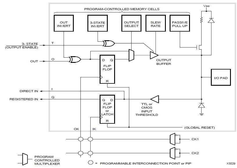
The XC3130A-3PC84C is a field programmable gate array (FPGA). The XC3130A-3PC84C provides a group of high-performance, high-density, digital integrated circuit. The XC3130A-3PC84C’s regular, extendable, flexible, user-programmable array architecture is composed of a configuration program store plus three types of configurable elements: a perimeter of I/O Blocks (IOBs), a core array of Configurable Logic Bocks (CLBs) and resources for interconnection. The development system provides schematic capture and auto place-and-route for design entry. Logic and timing simulation, and in-circuit emulation are available as design verification alternatives. The design editor is used for interactive design optimization, and to compile the data pattern that represents the configuration program.
Parametrics
XC3130A-3PC84C absolute maximum ratings: (1)Supply voltage relative to GND, VCC: -0.5 to +7.0 V; (2)Input voltage with respect to GND, VIN: -0.5 to VCC +0.5 V; (3)Voltage applied to 3-state output, VTS: -0.5 to VCC +0.5 V; (4)Storage temperature (ambient), TSTG: -65 to +150℃; (5)Maximum soldering temperature (10 s @ 1/16 in.), TSOL: +260℃; (6)Junction temperature plastic, TJ: +125℃; (7)Junction temperature ceramic, TJ: +150℃.
Features
XC3130A-3PC84C features: (1)Complete line of four related Field Programmable Gate Array product families, XC3000A, XC3000L, XC3100A, XC3100L; (2)Ideal for a wide range of custom VLSI design tasks: Replaces TTL, MSI, and other PLD logic; Integrates complete sub-systems into a single package; Avoids the NRE, time delay, and risk of conventional masked gate arrays; (3)High-performance CMOS static memory technology, Guaranteed toggle rates of 70 to 370 MHz, logic delays from 7 to 1.5 ns; System clock speeds over 85 MHz; Low quiescent and active power consumption; (4)Flexible FPGA architecture: Compatible arrays ranging from 1,000 to 7,500 gate complexity; Extensive register, combinatorial, and I/O capabilities; High fan-out signal distribution, low-skew clock nets; Internal 3-state bus capabilities; TTL or CMOS input thresholds; On-chip crystal oscillator amplifier; (5)Unlimited reprogrammability: Easy design iteration; In-system logic changes; (6)Extensive packaging options: Over 20 different packages; Plastic and ceramic surface-mount and pin-gridarray packages; Thin and Very Thin Quad Flat Pack (TQFP and VQFP) options; (7)Ready for volume production: Standard, off-the-shelf product availability; 100% factory pre-tested devices; Excellent reliability record; (8)Complete Development System: Schematic capture, automatic place and route; Logic and timing simulation; Interactive design editor for design optimization; Timing calculator; Interfaces to popular design environments like Viewlogic, Cadence, Mentor Graphics, and others.
Diagrams
| Image | Part No | Mfg | Description |  |
Pricing (USD) |
Quantity | ||||
|---|---|---|---|---|---|---|---|---|---|---|
 |
 XC3130A-3PC84C |
|
IC LOGIC CL ARRAY 3000GAT 84PLCC |
Data Sheet |
Negotiable |
|
||||
| Image | Part No | Mfg | Description | |
Pricing (USD) |
Quantity | ||||
|
XC31 |
Other |
|
Data Sheet |
Negotiable |
|
||||
|
XC3100 |
Other |
|
Data Sheet |
Negotiable |
|
||||
|
XC3100A |
Other |
|
Data Sheet |
Negotiable |
|
||||
|
XC3100L |
Other |
|
Data Sheet |
Negotiable |
|
||||
|
XC3120A-3PC68C |
|
IC LOGIC CL ARRAY 2000GAT 68PLCC |
Data Sheet |
Negotiable |
|
||||
|
XC3130A-3PC84C |
|
IC LOGIC CL ARRAY 3000GAT 84PLCC |
Data Sheet |
Negotiable |
|
||||