(Hong Kong)

Product Summary
The XC5202-6PC84C is a Field-Programmable Gate Array. The XC5202-6PC84C is engineered to deliver low cost. Building on experiences gained with three previous successful SRAM FPGA families, the device brings a robust feature set to programmable logic design. The VersaBlock. logic module, the VersaRing I/O interface, and a rich hierarchy of interconnect resources combine to enhance design flexibility and reduce time-to-market. Complete support for the XC5202-6PC84C is delivered through the familiar Xilinx software environment. The XC5202-6PC84C is fully supported on popular workstation and PC platforms.
Parametrics
XC5202-6PC84C absolute maximum ratings: (1)Supply voltage relative to GND, VCC: -0.5 to +7.0 V; (2)Input voltage with respect to GND, VIN: -0.5 to VCC +0.5 V; (3)Voltage applied to 3-state output, VTS: -0.5 to VCC +0.5 V; (4)Storage temperature (ambient), TSTG: -65 to +150℃; (5)Maximum soldering temperature (10 s @ 1/16 in. = 1.5 mm), TSOL: +260℃; (6)Junction temperature in plastic packages, TJ: +125℃; (7)Junction temperature in ceramic packages, TJ: +150℃.
Features
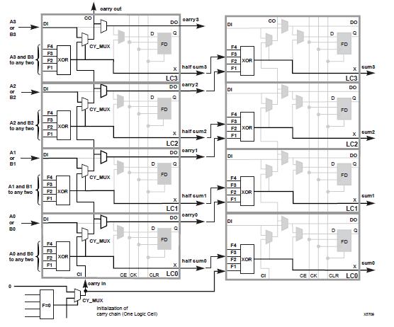
XC5202-6PC84C features: (1)Low-cost, register/latch rich, SRAM based reprogrammable architecture: 0.5mm three-layer metal CMOS process technology; 256 to 1936 logic cells (3,000 to 23,000 "gates"; Price competitive with Gate Arrays; (2)System Level Features, System performance beyond 50 MHz; 6 levels of interconnect hierarchy; VersaRing I/O Interface for pin-locking; Dedicated carry logic for high-speed arithmetic functions; Cascade chain for wide input functions; Built-in IEEE 1149.1 JTAG boundary scan test circuitry on all I/O pins; Internal 3-state bussing capability; Four dedicated low-skew clock or signal distribution nets; (3)Versatile I/O and Packaging, Innovative VersaRing I/O interface provides a high logic cell to I/O ratio, with up to 244 I/O signals; Programmable output slew-rate control maximizes performance and reduces noise; Zero Flip-Flop hold time for input registers simplifies system timing; Independent Output Enables for external bussing; Footprint compatibility in common packages within the XC5200 Series and with the XC4000 Series; Over 150 device/package combinations, including advanced BGA, TQ, and VQ packaging available; (4)Fully Supported by Xilinx Development System, Automatic place and route software; Wide selection of PC and Workstation platforms; Over 100 3rd-party Alliance interfaces; Supported by shrink-wrap Foundation software.
Diagrams
| Image | Part No | Mfg | Description |  |
Pricing (USD) |
Quantity | ||||
|---|---|---|---|---|---|---|---|---|---|---|
 |
 XC5202-6PC84C |
|
IC FPGA 64 CLB'S 84-PLCC |
Data Sheet |
Negotiable |
|
||||
| Image | Part No | Mfg | Description | |
Pricing (USD) |
Quantity | ||||
|
XC5200 |
Other |
|
Data Sheet |
Negotiable |
|
||||
|
XC5200 Series |
Other |
|
Data Sheet |
Negotiable |
|
||||
|
XC5202-5PQ100C |
|
IC - FPGA SPEED GRADE 5 COM TEMP |
Data Sheet |
Negotiable |
|
||||
|
XC5202-6PC84C |
|
IC FPGA 64 CLB'S 84-PLCC |
Data Sheet |
Negotiable |
|
||||
|
XC5202-6PQ100C |
|
IC FPGA 64 CLB'S 100-PQFP |
Data Sheet |
Negotiable |
|
||||
|
XC5204-5PC84C |
|
IC FPGA 120 CLB'S 84-PLCC |
Data Sheet |
Negotiable |
|
||||