(Hong Kong)


Product Summary
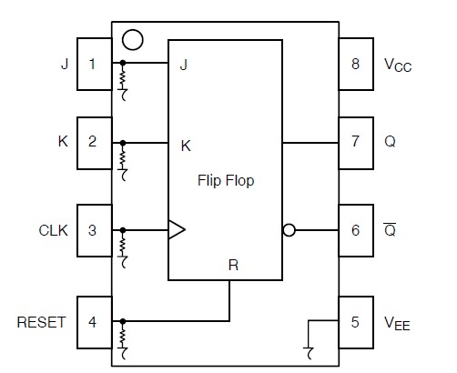
The MC100EP35DR2 is a higher speed/low voltage version of the EL35 JK flip−flop. The J/K data enters the master portion of the flip-flop when the clock is LOW and is transferred to the slave, and thus the outputs, upon a positive transition of the clock. The reset pin is asynchronous and is activated with a logic HIGH. The MC100EP35DR2 contains temperature compensation.
Parametrics
MC100EP35DR2 absolute maximum ratings: (1)VCC PECL Mode Power Supply VEE = 0 V: 6 V; (2)VEE NECL Mode Power Supply VCC = 0 V: -6 V; (3)VI PECL Mode Input Voltage: 6V; (4)NECL Mode Input Voltage: -6V; (5)Iout Output Current Continuous: 100mA; (6)TA Operating Temperature Range: -40 to +85 °C; (7)Tstg Storage Temperature Range: -65 to +150 °C.
Features
MC100EP35DR2 features: (1)410 ps Propagation Delay; (2)Maximum Frequency > 3 GHz Typical; (3)PECL Mode Operating Range: VCC = 3.0 V to 5.5 V with VEE = 0 V; (4)NECL Mode Operating Range: VCC = 0 V with VEE = -3.0 V to -5.5 V; (5)Open Input Default State; (6)Q Output Will Default LOW with Inputs Open or at VEE; (7)Pb-Free Packages are Available.
Diagrams
| Image | Part No | Mfg | Description |  |
Pricing (USD) |
Quantity | ||||||||||
|---|---|---|---|---|---|---|---|---|---|---|---|---|---|---|---|---|
 |
 MC100EP35DR2 |
ON Semiconductor |
Flip Flops 3.3V/5V ECL JK-Type |
Data Sheet |
Negotiable |
|
||||||||||
|
MC100EP35DR2G |
ON Semiconductor |
Flip Flops 3.3V/5V ECL JK-Type |
Data Sheet |
|
|
||||||||||