(Hong Kong)


Product Summary
The MC10EL35DR2 is a high speed JK flip-flop. The J/K data enters the master portion of the flip-flop when the clock is LOW and is transferred to the slave, and thus the outputs, upon a positive transition of the clock. The reset pin is asynchronous and is activated with a logic HIGH.
Parametrics
MC10EL35DR2 absolute maximum ratings: (1)VCC PECL Mode Power Supply VEE = 0 V: 8 to 0 V; (2)VEE NECL Mode Power Supply VCC = 0 V: -8 to 0 V; (3)VI PECL Mode Input Voltage VEE = 0 V VI ≤ VCC: 6 to 0V; (4)NECL Mode Input Voltage VCC = 0 V VI ≤ VEE: -6 to 0V; (5)Iout Output Current Continuous: 50mA; (6)Iout Output Current Surge: 100mA; (7)TA Operating Temperature Range: -40 to +85℃; (8)Tstg Storage Temperature Range: -65 to +150℃; (9)θJA Thermal Resistance (Junction to Ambient): 0 lpfm 190℃/W, 500 lpfm 130℃/W; (10)θJC Thermal Resistance (Junction to Case) Standard Board: 41 to 44 ℃/W; (11)Tsol Wave Solder Pb <2 to 3 sec @ 248℃: 265℃; (12)Tsol Wave Solder Pb-Free <2 to 3 sec @ 260℃: 265℃.
Features
MC10EL35DR2 features: (1)525 ps Propagation Delay; (2)2.2G Hz Toggle Frequency; (3)ESD Protection: > 1 kV Human Body Model, > 100 V Machine Model; (4)PECL Mode Operating Range: VCC = 4.2 V to 5.7 with VEE = 0 V; (5)NECL Mode Operating Range: VCC = 0 V with VEE = -4.2 V to; (6)-5.7 V; (7)Internal Input Pulldown Resistors on J, K, CLK, and R; (8)Meets or Exceeds JEDEC Spec EIA/JESD78 IC Latchup Test; (9)Moisture Sensitivity Level 1 For Additional Information, see Application Note AND8003/D; (10)Flammability Rating: UL-94 V-0 @ 0.125 in, Oxygen Index 28 to 34; (11)Transistor Count = 81 devices; (12)Pb-Free Packages are Available.
Diagrams
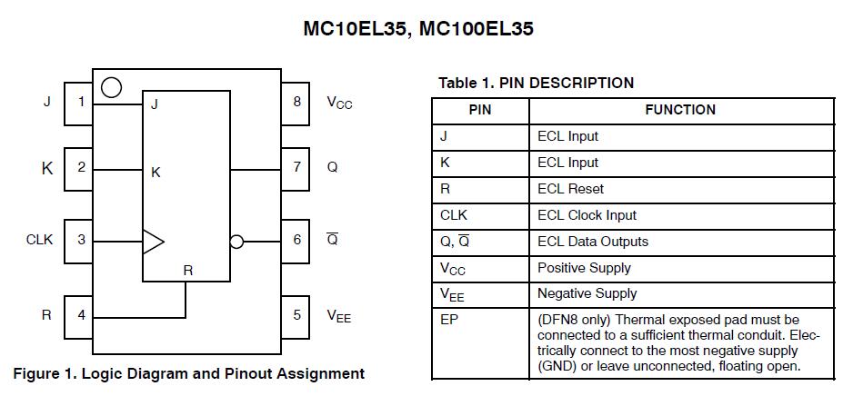
| Image | Part No | Mfg | Description |  |
Pricing (USD) |
Quantity | ||||||||||
|---|---|---|---|---|---|---|---|---|---|---|---|---|---|---|---|---|
 |
 MC10EL35DR2 |
ON Semiconductor |
Flip Flops 5V ECL JK-Type |
Data Sheet |
Negotiable |
|
||||||||||
|
MC10EL35DR2G |
ON Semiconductor |
Flip Flops 5V ECL JK-Type |
Data Sheet |
|
|
||||||||||