(Hong Kong)


Product Summary
The MC10EP05DR2 is a 2–input differential AND/NAND gate. The device is functionally equivalent to the EL05 and LVEL05 devices. With AC performance much faster than the LVEL05 device, the MC10EP05DR2 is ideal for applications requiring the fastest AC performance available.
Parametrics
MC10EP05DR2 absolute maximum ratings: (1)VCC PECL Mode Power Supply VEE = 0 V: 6 V; (2)VEE NECL Mode Power Supply VCC = 0 V: -6 V; (3)VI PECL Mode Input Voltage VEE = 0 V VI ≤ VCC: 6V; (4)NECL Mode Input Voltage VCC = 0 V VI ≥ VEE: -6V; (5)Iout Output Current Continuous: 50mA; (6)Iout Output Current Surge: 100mA; (7)IBB VBB Sink/Source: ± 0.5 mA; (8)TA Operating Temperature Range: -40 to +85 ℃; (9)Tstg Storage Temperature Range: -65 to +150 ℃; (10)θJA Thermal Resistance (Junction to Ambient): 0 lfpm 190℃/W, 500 lfpm 130℃/W; (11)θJC Thermal Resistance (Junction to Case): 41 to 44 ± 5% ℃/W; (12)Tsol Solder Temperature (<2 to 3 Seconds: 245℃ desired): 265℃.
Features
MC10EP05DR2 features: (1)170ps Typical Propagation Delay; (2)High Bandwidth to 3 Ghz Typical; (3)ECL mode: 0V VCC with VEE = ?.0V to ?.5V; (4)PECL mode: 3.0V to 5.5V VCC with VEE = 0V; (5)Internal Input Resistors: Pulldown on D, Pulldown and Pullup on D; (6)Q Output will default LOW with inputs open or at VEE; (7)ESD Protection: >4KV HBM, >200V MM; (8)New Differential Input Common Mode Range; (9)Moisture Sensitivity Level 1, Indefinite Time Out of Drypack. For Additional Information, See Application Note AND8003/D; (10)Flammability Rating: UL-94 code V-0 @ 1/8" Oxygen Index 28 to 34; (11)Transistor Count = 137 devices.
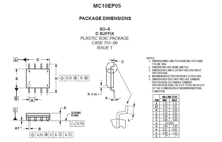
Diagrams
| Image | Part No | Mfg | Description |  |
Pricing (USD) |
Quantity | ||||||||||
|---|---|---|---|---|---|---|---|---|---|---|---|---|---|---|---|---|
 |
 MC10EP05DR2 |
|
IC GATE AND/NAND ECL 2INP 8-SOIC |
Data Sheet |
|
|
||||||||||
 |
MC10EP05DR2G |
ON Semiconductor |
Gates (AND / NAND / OR / NOR) 3.3V/5V ECL 2-Input Diff AND/NAND |
Data Sheet |
|
|
||||||||||