(Hong Kong)


Product Summary
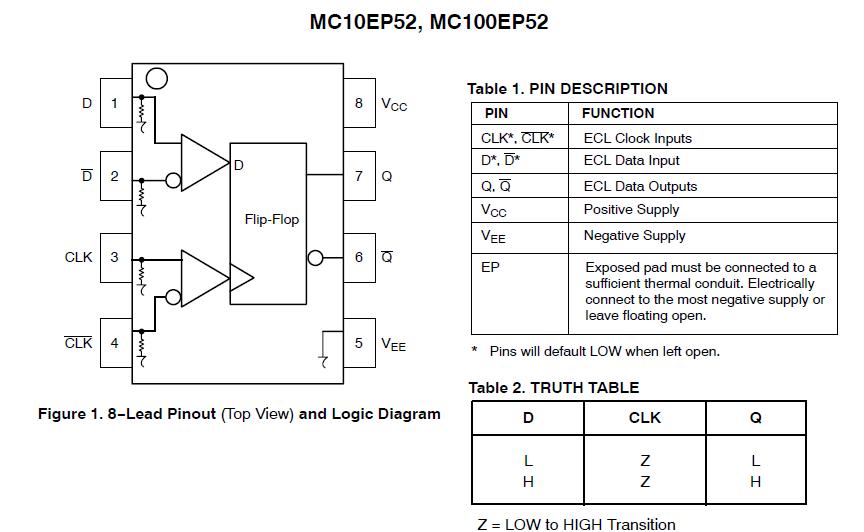
The MC10EP52DR2 is a differential data, differential clock D flip-flop. The device is pin and functionally equivalent to the MC10EP52DR2 device. Data enters the master portion of the flip-flop when the clock is LOW and is transferred to the slave, and thus the outputs, upon a positive transition of the clock. The differential clock inputs of the MC10EP52DR2 allow the device to also be used as a negative edge triggered device. The MC10EP52DR2 employs input clamping circuitry so that under open input conditions (pulled down to VEE) the outputs of the device will remain stable.
Parametrics
MC10EP52DR2 absolute maximum ratings: (1)VCC PECL Mode Power Supply VEE = 0 V: 6 V; (2)VEE NECL Mode Power Supply VCC = 0 V: -6 V; (3)VI PECL Mode Input Voltage VEE = 0 V VI ≤ VCC: 6V; (4)NECL Mode Input Voltage VCC = 0 V VI ≤ VEE: -6V; (5)Iout Output Current: Continuous 50mA, Surge 100mA; (6)IBB VBB Sink/Source: ± 0.5 mA; (7)TA Operating Temperature Range: -40 to +85 ℃; (8)Tstg Storage Temperature Range: -65 to +150 ℃; (9)θJA Thermal Resistance (Junction to Ambient): 0 lfpm 190℃/W, 500 lfpm 130℃/W; (10)θJC Thermal Resistance (Junction to Case) Standard Board: 41 to 44 ℃/W; (11)Tsol Wave Solder: Pb <2 to 3 sec @ 248℃ 265℃, Pb-Free <2 to 3 sec @ 260℃: 265℃.
Features
MC10EP52DR2 features: (1)330 ps Typical Propagation Delay; (2)Maximum Frequency > 4 GHz Typical; (3)PECL Mode: VCC = 3.0 V to 5.5 V with VEE = 0 V; (4)NECL Mode: VCC = 0 V with VEE = -3.0 V to -5.5 V; (5)Open Input Default State; (6)Safety Clamp on Inputs; (7)Q Output Will Default LOW with Inputs Open or at VEE; (8)Pb-Free Packages are Available.
Diagrams
| Image | Part No | Mfg | Description |  |
Pricing (USD) |
Quantity | ||||||||||
|---|---|---|---|---|---|---|---|---|---|---|---|---|---|---|---|---|
 |
 MC10EP52DR2 |
ON Semiconductor |
Flip Flops 3.3V/5V ECL D-Type |
Data Sheet |
Negotiable |
|
||||||||||
|
MC10EP52DR2G |
ON Semiconductor |
Flip Flops 3.3V/5V ECL D-Type Diff Data and Clock |
Data Sheet |
|
|
||||||||||