(Hong Kong)


Product Summary
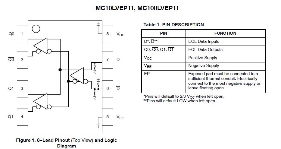
The MC10LVEP11DR2 is a differential 1:2 fanout buffer. The device is pin and functionally equivalent to the EP11 device. With AC performance the same as the EP11 device, the MC10LVEP11DR2 is ideal for applications requiring lower voltage. Single-ended CLK input operation is limited to a VCC ≥ 3.0 V in PECL mode, or VEE ≤ -3.0 V in NECL mode.
Parametrics
MC10LVEP11DR2 absolute maximum ratings: (1)VCC PECL Mode Power Supply VEE = 0 V: 6 V; (2)VEE NECL Mode Power Supply VCC = 0 V: -6 V; (3)VI PECL Mode Input Voltage VEE = 0 V VI ≤ VCC: 6V; (4)NECL Mode Input Voltage VCC = 0 V VI ≥ VEE: -6V; (5)Iout Output Current Continuous: 50mA; (6)Iout Output Current Surge: 100mA; (7)IBB VBB Sink/Source: ± 0.5 mA; (8)TA Operating Temperature Range: -40 to +85 ℃; (9)Tstg Storage Temperature Range: -65 to +150 ℃; (10)θJA Thermal Resistance (Junction to Ambient): 0 lfpm 190℃/W, 500 lfpm 130℃/W; (11)θJC Thermal Resistance (Junction to Case) Standard Board: 41 to 44 ℃/W; (12)Tsol Wave Solder Pb <2 to 3 sec @ 248℃: 265℃; (13)Tsol Wave Solder Pb- Free <2 to 3 sec @ 260℃: 265℃.
Features
MC10LVEP11DR2 features: (1)240 ps Typical Propagation Delay; (2)Maximum Frequency > 3.0 GHz Typical; (3)PECL Mode Operating Range: VCC = 2.375 V to 3.8 V with VEE = 0 V; (4)NECL Mode Operating Range: VCC = 0 V with VEE = -2.375 V to -3.8 V; (5)Open Input Default State; (6)Q Output Will Default LOW with Inputs Open or at VEE; (7)LVDS Input Compatible; (8)Pb-Free Packages are Available.
Diagrams
| Image | Part No | Mfg | Description |  |
Pricing (USD) |
Quantity | ||||||||||
|---|---|---|---|---|---|---|---|---|---|---|---|---|---|---|---|---|
 |
 MC10LVEP11DR2 |
ON Semiconductor |
Clock Buffer 2.5V/3.3V ECL 1:2 |
Data Sheet |
Negotiable |
|
||||||||||
|
MC10LVEP11DR2G |
ON Semiconductor |
Clock Buffer 2.5V/3.3V ECL 1:2 Diff Fanout Buffer |
Data Sheet |
|
|
||||||||||